

[ad_1]
Join day by day information updates from CleanTechnica on e-mail. Or comply with us on Google Information!
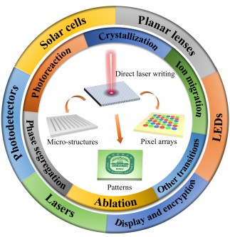
Steel halide perovskites have turn into well-deserved “star” supplies amongst a wide range of semiconductors owing to their wonderful optoelectronics properties, equivalent to excessive photoluminescence (PL) quantum yield (QY), excessive absorption coefficient, tunable bandgaps, lengthy provider diffusion lengths, and excessive defect tolerance, attracting huge consideration from each academia and business. In the meantime, DLW, primarily based on the interplay between mild and matter, is an environment friendly, contactless, masks free, and depth-resolved micro-patterning approach. It’s usually carried out by coupling a laser beam with a high-resolution microscope to reduce the output focal spot. The decision of DLW depends on the diameter of the output focal spot and the brink response of the fabric. Relying on the fabrication mechanisms and materials threshold responses, one of the best decision is normally between a pair to some a whole lot of nanometers. The analysis on DLW additionally deepens the basic understanding on the interplay mechanisms between mild and perovskites, paving the best way for designing optoelectronic units with improved performances.
In a evaluate paper (https://doi.org/10.37188/lam.2024.004) printed in Mild Superior & Manufacturing, a crew of scientists, led by Professor Zhixing Gan from Middle for Future Optoelectronic Practical Supplies, Nanjing Regular College, China, and colleagues have summarized latest analysis progress of DLW on perovskites. The concrete interplay mechanisms between laser and perovskite are categorized into six components, together with laser ablation, laser induced crystallization, laser induced ion migration, laser induced section segregation, laser induced photoreaction, and different laser induced transitions. Then, they give attention to the purposes of those perovskites with micro/nano patterns and array constructions, equivalent to show, optical info encryption, photo voltaic cells, LEDs, laser, photodetectors, and planar lenses. Some great benefits of the patterned constructions are highlighted. Lastly, present challenges for DLW on perovskites are outlooked and views on their future developments are additionally put ahead.
Laser is a superb software to control, fabricate and course of nano-/micro-structures on semiconductors with distinctive benefits of excessive precision, contactless, straightforward operation, masks free. DLW primarily based on totally different interplay mechanisms between laser and perovskites have been developed because of the particular construction of perovskites. The detailed interplay mechanism sensitively relies on laser, equivalent to wavelength, pulse/CW, energy, and repetition charge, due to this fact offering a versatile and highly effective software to course of the perovskites with exactly managed nano- or micro-structures. The wide range of interplay mechanisms decide the DLW’s nice potential for numerous purposes in microelectronics, photonics and optoelectronics.
Cheaper and flexibly controllable fabrication lasers, along with perovskite’s superior optoelectronic properties will convey nice software potential for DLW on perovskites. Presently it’s nonetheless within the infancy stage, anticipating an enormous growth in each basic analysis and business demand within the close to future. For the long run growth of DLW on perovskites, some essential technical bottlenecks must be solved, such because the decision of DLW approach, the present time of segregated phases, and the micropatterning approach to versatile substrates, and many others. The purposes of perovskites nearly cowl all types of optoelectronic and photonic areas, equivalent to single photon supply, micro/nano lasers, photo-detectors, optical gates, optical communication, waveguide, and nonlinear optics. Thus, it is extremely promising to assemble and combine photonic units with totally different features primarily based on a single perovskite chip.
Funding info
This work was supported by the Pure Science Basis of Shandong Province (ZR2021YQ32), the Taishan Scholar Undertaking of Shandong Province (tsqn201909117), the Nationwide Pure Science Basis of China (Nos. 61901222, 21802074 and 11604155), Pure Science Basis of Jiangsu Province (BK20190697).
Have a tip for CleanTechnica? Need to promote? Need to counsel a visitor for our CleanTech Speak podcast? Contact us right here.
Newest CleanTechnica TV Video

CleanTechnica makes use of affiliate hyperlinks. See our coverage right here.
[ad_2]